First of all, I
would like to “memaparkan” what is all about designing the hardware of SHA-1.
Based on the algorithm discussed in section A, it is defined that the length of
the input to SHA-1, which has been translated in the form of a sequence of
binary numbers, ranges from 0 to 264 bits long. It is, of course,
easy to receive an arbitrary input with any number of length enclosed within the
range by implementing SHA-1 in the form of software, regardless of how complex
the program is, such as the C program shown in section B, that is made by NIST
in USA. This is because any kind of software programming usually provides some
kind of looping facility which makes
it easy to repeat the same action, which is,in this case, receiving input bits,
for some period of times. On the other hand, a digital hardware implementation,
especially, of SHA-1 has its own unique way to handle the input. It uses a
component called a register. The term “component” in the hardware
implementation is analogous to a subprogram in the software implementation.
Register is designed to receive and keep temporarily and then output the n-bit
data. In this case, n is an integer that is usually more than 0 and as long as I
have known so far, no convention limits the number of n in designing the
register which is so called n-bit register. However, speaking about the input of
SHA-1 which I am designing with VHDL in my final assignment, I think that I
won’t be capable to realize a structural 264-bit register which
will be synthesized later, in order to handle the current input to SHA-1. I just
can’t imagine that. Therefore, I take a tricky way to build up SHA-1 in the
form of hardware, of which operation is not against to the original algorithm
which have to be followed. I perform the mechanism of SHA-1’s operation when
implemented in a hardware as follows. As a sequence of bits having an arbitrary
length (which is still in the range of 0 to 264 bit) become an input
to SHA-1, a digital hardware of SHA-1 will receive per n bits of the current
input, and directly process them to become 160-bit ouput which is then known as
a message digest. In other word, I would say that, the first thing that has to
be done by a digital hardware of SHA-1 is receiving the first n bits sequence of
the current input and then processing them to produce a 160-bit message digest.
After producing the first 160-bit message digest, the digital hardware of SHA-1
again receives the second n bits sequence of
the current input, and processes them to produce the second 160-bit
message digest. This result is next followed by the same action to produce the
third 160-bit message digest. This action done by SHA-1 will be repeated over
again, which seems to me like a cycle, till the last n sequence of the current
input to produce the last 160-bit message digest.
In order to
realize the mechanism in the digital hardware of SHA-1, it is necessary for me
to first say that, the number of n which is mentioned above to be an integer
more than 0, is dependent on the designer to decide. In this case, I decide the
number of n to be 24 meaning that the digital hardware of SHA-1 will receive and
process per 24 bit sequence of a current input at a time to produce its related
160-bit message digest. Consequently, I must set to design such a 24-bit
register in VHDL so that it can help SHA-1 run the operation in the mechanism I
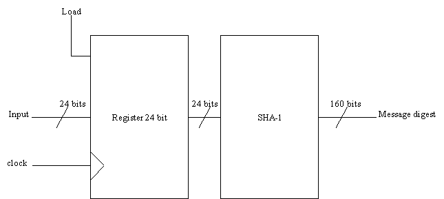
want it to perform. The block diagram of the
digital hardware of SHA-1 based on
my designing version can be seen in the figure below.
The block diagram
figured above operates the mechanism process explained in the first paragraph,
just as what I want it to perform. When some sequence of
data bits to be processed becomes input to SHA-1, the earlier 24 bits
sequence of the data bits gets simultaneously (pararellelly) in the input of the
24-bit register, then it will be held there till the Load of the
register turns to be in the logical value (state) 1 from the state 0. It is
because when the logical value of the
Load turns to be 1, the input in the register will be connected to its output
simultaneously and, of course, it also means that the earlier 24 bit sequence of
the data bits in the input will be transferred to the output
in the next rising edge of the
clock. As the input is connected to the ouput, the Load’s logical value will
instaneously change to be 0 which means that the register holds the next 24 bit
sequence of the data in the input
for some certain period of time which SHA-1 takes to produce 160-bit message
digest. This action of the SHA-1 will be repeated over and over again till the
last 24-bit sequence of the current data bits.
Finally, this is it for this time. And I will explain more about the external component that controls the change of the state in the Load of the register and the internal components of the SHA-1 in the updated information of mine later. So, thank you for having read this information and I expect to have inputs and more inspiration about this.